Welcome to SCHOTT
As a global material technology group and one of the leading specialty glass companies in the world, it’s our purpose to pioneer the impossible for a better future.
Discover our purpose
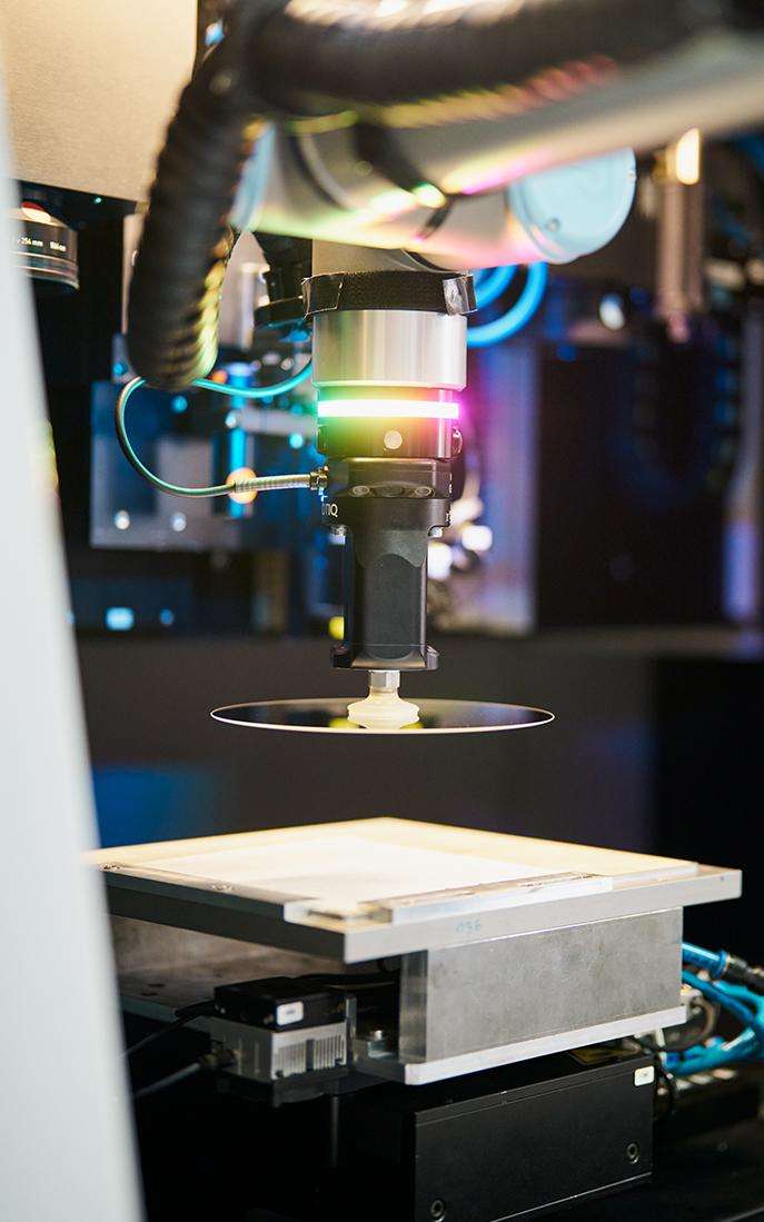
Our expertise
140 years of experience in creating groundbreaking glass solutions evolved into our commitment to material innovations. Discover how SCHOTT uses this unique know-how and the latest technology to set new standards in a wide range of industries.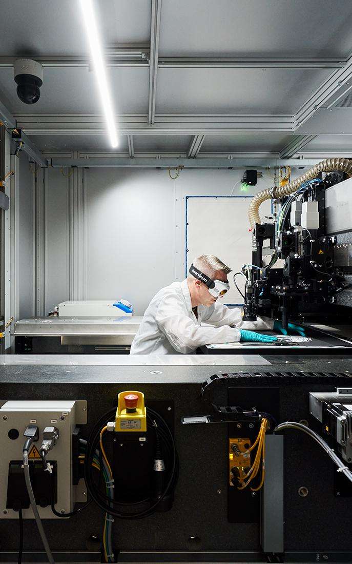
Careers at SCHOTT
Learn about the career opportunities and benefits waiting for you at one of the leading international technology groups in the areas of specialty glass, glass-ceramics and material solutions. At SCHOTT everybody can make a difference. Because together, we pioneer groundbreaking glass and material innovations, fueling science and inspiring progress.
Projects and references
From protecting ancient manuscripts to expanding our knowledge of the universe: SCHOTT has a long history of working with world’s leading specialists, using our expertise in glass and material technology to solve complex challenges.